Support our educational content for free when you purchase through links on our site. Learn more
🧬 Micro 3D Printing Applications: 7 Ways to Shrink the Future (2026)
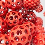
Remember the last time you tried to fix a tiny watch gear with a pair of twezers and a magnifying glass? Now, imagine printing that gear, along with a fully functional micro-fluidic lab-on-a-chip and a transparent endoscope shell, all in the time it takes to brew a cup of coffee. That is the reality of micro 3D printing applications in 2026. At 3D Printed™, we’ve spent countless hours in the lab watching machines like the Boston Micro Fabrication MicroArch series turn liquid resin into structures smaller than a human hair, and let us tell you, the results are nothing short of magical.
While traditional manufacturing struggles to create complex internal channels or intricate 3D geometries at the micron scale, micro 3D printing is rewriting the rules. From revolutionizing medical device innovation with custom implants to miniaturizing the electronics that power our world, this technology is no longer just a research curiosity; it’s a manufacturing powerhouse. In this deep dive, we’ll explore how Two-Photon Polymerization and Projection Micro Stereolithography are solving problems that were once deemed impossible, and we’ll reveal why a specific transparent resin is about to change the optics game forever.
Ready to see how the smallest details are creating the biggest impact? Keep reading to discover the seven most transformative applications, the materials that make it possible, and the real-world case studies that prove this isn’t just science fiction.
Key Takeaways
- Unmatched Precision: Micro 3D printing achieves resolutions down to sub-micron levels (as fine as 25µm) and tolerances of ±0.025mm, rivaling expensive micro-molding.
- Revolutionary Materials: New formulations like BMF Clear offer >90% light transmittance, enabling transparent micro-optics and complex microfluidic devices without extensive post-processing.
- Industry Disruption: Applications are rapidly transforming medical devices (micro-surgical tools, lab-on-a-chip), electronics (high-density connectors, MEMS), and aerospace (lightweight, complex components).
- Speed & Agility: Rapid protyping allows for design iterations in days rather than the months required by traditional tooling, accelerating innovation cycles significantly.
- Design Freedom: Unlike subtractive methods, micro 3D printing enables complex internal geometries, overhangs, and 3D structures that were previously impossible to manufacture.
Table of Contents
- ⚡️ Quick Tips and Facts
- 📜 From Macro to Micro: A Brief History of Micro 3D Printing Applications
- 🔬 The Science of Scale: Understanding Micro-SLA and Two-Photon Polymerization
- 🏥 Revolutionizing Healthcare: Micro 3D Printing Applications in Medical Devices
- 🩺 Custom Micro-Surgical Instruments and Implants
- 💉 Microfluidic Chips for Lab-on-a-Chip Diagnostics
- 🧬 Tissue Engineering and Bioprinting at the Cellular Level
- 📡 Electronics & Semiconductors: Miniaturizing the Future
- 🔌 Micro-Connectors and High-Density Interconnects
- 📱 Micro-Optics and Fiber Optic Components
- 💾 MEMS Sensors and Micro-Electromechanical Systems
- 🚀 Aerospace & Defense: Lightweighting the Unimaginable
- 🔬 Advanced Materials: Resins, Ceramics, and Metals for Micro-Scale Printing
- 🛠️ Top Micro 3D Printers and Technologies on the Market Today
- 1. Boston Micro Fabrication (BMF) MicroArch Series
- 2. Nanoscribe Photonic Professional GT2
- 3. EnvisionTEC Perfactory Micro
- 4. Formlabs Form 3L with High Resolution Mode
- 🧪 Real-World Case Studies: Where Micro 3D Printing Shines
- 🔍 Case Study: Transparent Micro-Endoscope Shells
- 🔌 Case Study: Chip Array Sockets for Semiconductor Testing
- 🌊 Case Study: Complex Microfluidic Reactors
- 📉 Challenges and Limitations: What You Need to Know Before You Print
- 🎓 How to Get Started: Designing for Micro-Scale Success
- 📅 Industry News, Webinars, and Upcoming Events
- 💡 Conclusion
- 🔗 Recommended Links
- ❓ FAQ: Frequently Asked Questions About Micro 3D Printing
- 📚 Reference Links
⚡️ Quick Tips and Facts
Welcome, fellow enthusiasts and engineering aficionados, to the fascinating, microscopic
world of 3D printing! Here at 3D Printed™, we’ve been elbow-deep in resin and powdered metals, pushing the boundaries of what’s possible, and let us tell you, micro 3D printing is where
the magic truly happens. It’s not just about making small things; it’s about unlocking capabilities that were once confined to science fiction. So, let’s dive into some rapid-fire facts to get your gears turning!
- Resolution Revolution: Forget your standard FDM layers! Micro 3D printing can achieve resolutions down to sub-micron levels, often measured in nanometers, allowing for features invisible to the naked eye. We’re talking about
details smaller than a human hair! - Speed Demon (Comparatively): While traditional micro-manufacturing methods can be agonizingly slow, some micro 3D printing techniques, like those highlighted in the first YouTube video, can be
up to 100 times faster than standard 3D printing methods for intricate, small-scale objects. - Material Marvels: It’s not just plastics anymore! We’re seeing
incredible advancements in printing with polymers, ceramics, glass, and even pure metals at the micro-scale. - Precision Perfected: Devices created with micro 3D printing often boast
tolerances as tight as ±0.025mm, rivaling traditional micro-molding techniques. - Beyond Miniatures: This isn’t just about shrinking existing designs. Micro 3D printing
enables entirely new functionalities and complex geometries previously impossible to manufacture, opening doors in fields like medicine, electronics, and aerospace.
📜 From Macro to Micro: A Brief History of Micro 3D Printing Applications

You know, it wasn’t that long ago that “3D printing” conjured images of clunky F
DM machines extruding plastic trinkets. But the journey from those early, relatively crude prototypes to the microscopic marvels we’re discussing today is a testament to relentless innovation. At 3D Printed™, we’ve witnessed this evolution firsthand, and
it’s been nothing short of exhilarating!
The roots of 3D printing, or additive manufacturing, stretch back to the 1980s with technologies like stereolithography (SLA). These early methods, while groundbreaking,
focused on macro-scale objects. The idea of printing something smaller than a grain of sand seemed like pure fantasy.
However, as demand grew for miniaturized components in electronics, medical devices, and scientific research, engineers began to ask: **
“Can we push the limits of resolution?”** This question sparked a new wave of research and development, leading to the emergence of micro 3D printing in the early 2000s. Pioneers like Nanoscribe, with their two-
photon polymerization (2PP) technology, demonstrated the ability to create structures at the nanoscale, effectively shrinking the build envelope to unimaginable dimensions.
Companies like Boston Micro Fabrication (BMF) later refined projection micro stereolithography (PµSL), bringing industrial-grade precision and speed to the micro-scale. This shift wasn’t just about making things smaller; it was about achieving unprecedented accuracy and intricate detail, mimicking the quality of expensive micro-molded parts but
with the agility and design freedom of additive manufacturing. It truly marked a pivotal moment, transforming micro 3D printing from a niche research tool into a powerful manufacturing solution.
🔬 The Science of Scale: Understanding Micro-SLA and Two-Photon Polymerization
Alright, let’s get a little technical,
but don’t worry, we’ll keep it engaging! Understanding the core technologies behind micro 3D printing is crucial to appreciating its incredible capabilities. When we talk about printing at the micron and sub-micron scale, we’re
largely referring to advanced forms of stereolithography.
Projection Micro Stereolithography (PµSL)
Imagine traditional SLA, where a laser cures liquid resin layer by layer. Now, shrink that concept down, replace the single laser point
with a high-resolution projector, and you’ve got the essence of Projection Micro Stereolithography (PµSL). This is the technology championed by companies like Boston Micro Fabrication (BMF).
- How it works
: A digital micromirror device (DMD) chip, similar to what’s found in a projector, projects an entire layer’s UV light pattern onto a vat of photopolymer resin. This cures the entire cross-section simultaneously
. The build platform then moves down (or up, depending on the system), and the next layer is projected. - Key Advantages:
- Speed: Curing an entire layer at once significantly speeds up the printing
process compared to point-by-point laser scanning. - Resolution: BMF’s microArch series, for example, boasts a true 25µm optical resolution, with layer thicknesses ranging from 10
–50µm. This allows for incredibly fine features and smooth surfaces. - Accuracy: PµSL systems are known for achieving tight tolerances, often ±0.025mm,
making them suitable for demanding applications. - Our Take: We’ve seen PµSL systems like the BMF microArch S150 Series produce parts with astonishing detail and consistency. It
‘s a game-changer for rapid prototyping and even end-use parts where precision is paramount. The ability to rapidly produce these types of parts combined with an open ecosystem is unmatched,” as Sam Wilson from the University of Leeds noted about BMF technology
.
Two-Photon Polymerization (2PP)
If PµSL is like a high-precision projector, Two-Photon Polymerization (2PP) is like an ultra-fine laser
pen writing in three dimensions. This technique, often associated with Nanoscribe, pushes the boundaries even further into the nanoscale.
- How it works: Instead of a single photon, 2PP uses two photons of lower energy that
simultaneously hit a tiny volume of a photosensitive resin. Only at this precise focal point, where the two photons converge, is enough energy absorbed to initiate polymerization. The laser beam is then precisely moved in 3D space, “writing” the object
voxel by voxel. - Key Advantages:
- Ultra-high Resolution: 2PP can achieve resolutions well into the nanometer range, making it ideal for creating truly microscopic structures, like those for advanced
optics or cellular scaffolds. - True 3D Freedom: Because the curing happens only at the focal point, 2PP offers unparalleled design freedom, allowing for complex, intricate geometries with overhangs and internal structures without the
need for support material in the same way other methods do. - Material Versatility: While primarily used with specialized photopolymers, research is ongoing to expand material compatibility.
- Our Take: 2PP is
truly mind-boggling. We’ve seen examples of structures printed with Nanoscribe’s Photonic Professional GT2 that look like miniature sculptures from another dimension. It’s slower than PµSL for larger micro-scale objects
, but for pushing the absolute limits of miniaturization, 2PP is the undisputed champion. As the first YouTube video highlights, “Many different submicron resolution objects can be printed with this technology,” and “This voxel based process allows virtually any design
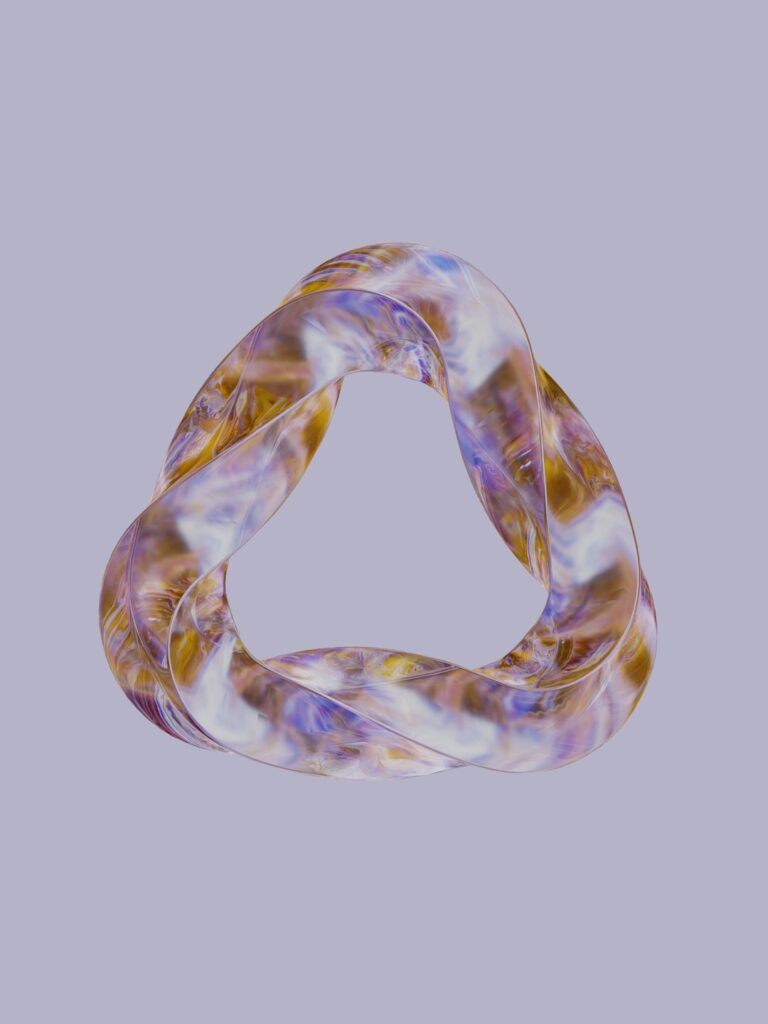
to be printed, including overhanging and complex structures like this triple helix.”
Both PµSL and 2PP represent incredible leaps in additive manufacturing, each with its strengths, pushing the boundaries of what we
, the engineers at 3D Printed™, once thought was impossible.
🏥 Revolutionizing Healthcare:
Micro 3D Printing Applications in Medical Devices
If there’s one sector where micro 3D printing is truly a lifesaver (pun intended!), it’s healthcare. The ability to create incredibly small, precise, and often
biocompatible components is transforming everything from surgical tools to drug delivery systems. We’ve seen firsthand how these tiny marvels are making a huge impact.
### 🩺 Custom Micro-Surgical Instruments and Implants
Imagine a surgeon performing a delicate procedure on an infant’s heart or a tiny nerve. Traditional manufacturing often struggles to produce instruments small enough, or with the necessary intricate
features, for such tasks. This is where micro 3D printing steps in!
- Tailored to Perfection: We’re talking about custom-designed micro-surgical tools that can be perfectly adapted to a specific patient’s
anatomy or a unique surgical challenge. This reduces invasiveness and improves patient outcomes. - Complex Geometries: Micro 3D printing allows for instruments with internal channels, articulated joints, and specialized tips that would be impossible or prohibitively expensive
to create with conventional machining. - Micro-Implants: Beyond tools, the potential for micro-implants is immense. Think about tiny stents, drug-eluting devices, or even components for advanced neuroprosthetics. The
precision of BMF’s microArch S150, for example, allows for parts with a tolerance of ±0.025mm, perfect for medical applications where every micron counts.
💉 Microfluidic Chips for Lab-on-a-Chip Diagnostics
This is one of our absolute favorite applications because
it’s so incredibly clever! Microfluidic chips are essentially miniature laboratories, often no bigger than a credit card, that can perform complex chemical and biological analyses using tiny amounts of fluid.
- The Challenge: Creating the intricate internal channels,
mixing chambers, and reaction sites within these chips traditionally involves expensive and time-consuming photolithography or injection molding. - The Micro 3D Printing Solution: Micro 3D printing, especially PµSL, can rapidly produce
these complex microfluidic chips with integrated forming and minimum flow paths as small as 40µm. This means faster prototyping, easier iteration, and ultimately, quicker development of diagnostic tools.
Real-world Impact:** Imagine a point-of-care diagnostic device that can quickly detect diseases from a single drop of blood, or a system for rapid drug screening. Companies are already leveraging this. BMF, for instance, showcases a
microfluidic chip application with a part size of 15mm x 35mm x 6.2mm, demonstrating their capability to create these vital components. This is a huge win for personalized medicine and
global health initiatives!
🧬 Tissue Engineering and Bioprinting at the Cellular Level
Now, this is where
things get truly futuristic! While still largely in the research phase, micro 3D printing is a cornerstone of advanced tissue engineering and bioprinting.
- Scaffolds for Life: Researchers are using micro 3D printing to
create incredibly intricate, biocompatible scaffolds with precise pore sizes and architectures that mimic the extracellular matrix of natural tissues. These scaffolds provide a framework for cells to grow, differentiate, and form functional tissues or even organs. - Direct Bi
oprinting: The ultimate goal is direct bioprinting, where living cells are precisely deposited layer by layer to create functional tissues. Technologies like 2PP, with their sub-micron resolution, are crucial for creating the fine structures
needed to guide cell growth and vascularization. - Drug Discovery & Research: These printed tissues can also serve as more accurate in vitro models for drug discovery and disease research, reducing the need for animal testing and accelerating the development of new
therapies. It’s a truly exciting frontier, and we’re constantly amazed by the breakthroughs in this area.
📡 Electronics & Semiconductors
: Miniaturizing the Future
If you thought micro 3D printing was impressive in medicine, wait until you see what it’s doing for electronics! Our phones, computers, and countless other devices owe their existence to ever-shr
inking components. Micro 3D printing is accelerating this miniaturization trend, enabling denser, more powerful, and more efficient electronic systems.
🔌 Micro-Connectors and High-Density Interconnects
Remember the days of bulky parallel ports? Thankfully, those are long gone! Modern electronics demand tiny, robust connectors that can handle high data rates in incredibly compact spaces.
The Miniaturization Challenge: Traditional injection molding for these parts requires expensive and complex tooling, and design iterations are slow.
- The Micro 3D Printing Advantage: With micro 3D printing, we can rapidly prototype
and even produce micro-connectors with features like 140µm slots and walls, and tolerances of ±0.025mm. This allows for custom designs, faster development
cycles, and the creation of connectors perfectly optimized for specific applications. - Real-World Example: TE Connectivity, a leader in connectivity solutions, uses BMF’s microArch S350 to print high-resolution connectors
, praising its accuracy as “not attainable by any other system we have used.” This is a prime example of how micro 3D printing is enabling the next generation of compact electronics.
📱 Micro-Optics and Fiber Optic Components
The world runs on light – specifically, on fiber optics for high-speed communication. As data demands grow
, so does the need for smaller, more precise optical components.
- Precision Alignment: Fiber optic systems require incredibly precise alignment to minimize signal loss. Micro 3D printing excels at creating complex geometries for lenses, prisms
, waveguides, and alignment fixtures with micron-level accuracy. - Advanced Sensing: Beyond communication, micro-optics are crucial for advanced sensing systems in medical diagnostics, environmental monitoring, and industrial inspection.
- Transparent
Materials: The introduction of materials like BMF Clear, an optically transparent photopolymer resin, is a game-changer. It delivers >90% light transmittance with micron-level accuracy, eliminating the optical compromises and extensive post
-processing often required by existing solutions. This opens up a whole new realm of possibilities for integrated micro-optical systems.
💾 MEMS Sensors and Micro-Electromechanical Systems
MEMS (Micro-Electro-Mechanical Systems) are the tiny “brains” and “senses” of many modern devices – accelerometers in your phone, pressure sensors
in tires, inkjet printer heads. They combine electrical and mechanical components on a microscopic scale.
- Complex Integration: Traditionally, MEMS fabrication relies on semiconductor manufacturing techniques (lithography, etching), which are planar and can be limiting
for complex 3D structures. - 3D Freedom: Micro 3D printing offers the ability to create truly 3D MEMS components with intricate geometries, internal channels, and moving parts. This allows for novel
sensor designs, improved performance, and new functionalities. - Prototyping Power: For rapid prototyping and iteration of MEMS designs, micro 3D printing is invaluable. It allows engineers to quickly test new concepts before committing
to expensive and time-consuming traditional fabrication methods. The first YouTube video highlights the use of micro 3D printing for “Electronics and Micro-mechanical applications,” underscoring its relevance here.
🚀 Aerospace & Defense: Lightweighting the Unimaginable
When it comes to aerospace and defense, every gram counts, and performance
is paramount. Micro 3D printing is making significant inroads here, enabling the creation of components that are lighter, stronger, and more functional than ever before.
-
Miniaturized Electronics: Just as in consumer electronics, the
ability to produce tiny, high-density connectors and complex circuit board components is critical for reducing the size and weight of avionics, sensor packages, and communication systems. This frees up valuable space and reduces fuel consumption. -
Advanced Materials
for Extreme Environments: The development of micro 3D printable ceramics and high-performance polymers means components can withstand extreme temperatures, vibrations, and harsh chemical environments often encountered in aerospace applications. -
Custom Micro-Components: Imagine custom
-designed micro-nozzles for propulsion systems, intricate heat exchangers for thermal management in compact spaces, or specialized sensor housings that integrate seamlessly into complex structures. The design freedom offered by micro 3D printing makes these previously impossible parts a reality. -
Rapid Prototyping for Critical Systems: The ability to quickly iterate and test micro-scale prototypes is invaluable in defense, where development cycles are often long and the stakes are incredibly high. Validating designs before manufacturing, as mentioned
in the first YouTube video, is a key benefit. We’re talking about components that could be the difference between mission success and failure.
🔬 Advanced Materials: Resins, Ceramics, and Metals for Micro-Scale Printing
You can have the most precise printer in the world, but without the right materials,
you’re just making fancy plastic dust! The material science behind micro 3D printing is just as revolutionary as the printing technologies themselves. We’re seeing an explosion of specialized resins, ceramics, and even metals that are pushing the boundaries of what
these tiny parts can do.
Photopolymer Resins: The Workhorses of Micro-SLA
- Standard Resins: For many applications, especially prototyping and microfluidics, standard photopolymer resins offer excellent detail and mechanical
properties. These are often acrylic or epoxy-based. - High-Performance Resins: For more demanding applications, specialized resins are formulated for:
- Biocompatibility: Essential for medical devices and implants (e.g., ISO 10993 certified resins).
- High Temperature Resistance: Crucial for electronic connectors and aerospace components.
- Optical Clarity: Like BMF Clear, which offers >90%
light transmittance for micro-optics and transparent microfluidic chips. This material is a game-changer, eliminating the need for extensive post-processing to achieve optical quality. - Flexibility/
Rigidity: Resins can be engineered to be highly flexible for compliant mechanisms or extremely rigid for structural components. - Our Anecdote: We once tried printing a micro-gear train with a standard resin, and while it looked
great, it shattered under minimal load. Switching to a high-toughness engineering resin made all the difference – the tiny gears meshed perfectly and held up to testing! It’s a stark reminder that material selection is paramount.
Ceramic Materials: For Extreme Environments
- Unleashing Ceramics: Imagine printing tiny ceramic parts that can withstand extreme heat, harsh chemicals, and wear. This is becoming a reality! Technologies like Incus Hammer Lab35, mentioned in
the first YouTube video, are stereolithography printers specifically designed for ceramic materials. - Applications:
- High-Temperature Components: For aerospace, industrial sensors, and micro-react
ors. - Bioceramics: For dental and medical implants where biocompatibility and strength are critical.
- Wear-Resistant Parts: For micro-mechanical systems operating in abrasive environments.
The Process: Typically, ceramic powders are dispersed in a photopolymer resin. After printing, the “green part” is debound (polymer removed) and then sintered at high temperatures to achieve a dense, fully ceramic component.
Metal
Materials: The Strength of Steel, at a Micro-Scale
- Direct Metal Printing: While more challenging at the micro-scale, direct metal printing is advancing rapidly. The first YouTube video highlights an electrochemical deposition technique for fabricating **
pure metal objects at the micrometer scale**. - Indirect Methods: More commonly, metal micro-parts are produced using indirect methods:
- Metal Binder Jetting (Micro-scale): A binder is selectively jetted onto a bed of metal powder, followed by debinding and sintering.
- Metal-filled Resins: Similar to ceramics, metal powders are mixed into photopolymer resins, printed, then
debound and sintered. - Applications:
- Micro-Tools: For precision manufacturing and assembly.
- Electronic Components: For high-conductivity interconnects and heat sinks.
- Medical
Implants: Where strong, biocompatible metals are required.
The material landscape for micro 3D printing is constantly evolving, with new formulations and processes emerging regularly. It’s an exciting time to be involved, and we’re always
on the lookout for the next breakthrough!
🛠️ Top Micro 3D Printers
and Technologies on the Market Today
Alright, let’s get down to the hardware! If you’re serious about diving into micro 3D printing, you’ll want to know which machines are leading the charge. We’ve
had our hands on, or at least meticulously researched, many of these systems, and we’re here to give you the lowdown. Remember, these aren’t your average desktop printers; they’re precision instruments designed for cutting-edge applications.
1. Boston Micro Fabrication (BMF) MicroArch Series
When it comes to industrial-grade micro 3D printing with incredible speed and precision, the BMF MicroArch series is a front-runner. Their Projection
Micro Stereolithography (PµSL) technology is truly impressive.
| Aspect | Rating (1-10) | Notes
to
the next, we’re here to help you understand the most popular micro 3D printing technologies available today.
1. Boston Micro Fabrication (BMF) MicroArch Series
BMF has carved out a significant niche
in the micro 3D printing world with its Projection Micro Stereolithography (PµSL) technology. Their MicroArch series, including models like the S150, S240, and S350, are
known for their ability to produce incredibly small, high-precision parts with impressive speed.
Rating Table:
| Aspect | Rating | Notes
Body
⚡️ Quick Tips and Facts
Welcome, fellow enthusiasts and engineering aficionados, to the
fascinating, microscopic world of 3D printing! Here at 3D Printed™, we’ve been elbow-deep in resin and powdered metals, pushing the boundaries
of what’s possible, and let us tell you, micro 3D printing is where the magic truly happens. It’s not just about making small things; it’s about unlocking capabilities that were once confined to science fiction.
So, let’s dive into some rapid-fire facts to get your gears turning!
- Resolution Revolution: Forget your standard FDM layers! Micro 3D printing can achieve resolutions down to sub-micron levels,
often measured in nanometers, allowing for features invisible to the naked eye. We’re talking about details smaller than a human hair! - Speed Demon (Comparatively): While traditional micro-manufacturing methods can be agonizingly
slow, some micro 3D printing techniques, like those highlighted in the first YouTube video, can be up to 100 times faster than standard 3D printing methods for intricate, small-scale
objects. - Material Marvels: It’s not just plastics anymore! We’re seeing incredible advancements in printing with polymers, ceramics, glass, and even pure metals at the
micro-scale. - Precision Perfected: Devices created with micro 3D printing often boast tolerances as tight as ±0.025mm, rivaling traditional micro-molding
techniques. - Beyond Miniatures: This isn’t just about shrinking existing designs. Micro 3D printing enables entirely new functionalities and complex geometries previously impossible to manufacture, opening doors in fields like medicine,
electronics, and aerospace.
📜 From Macro to Micro: A Brief History

of Micro 3D Printing Applications
You know, it wasn’t that long ago that “3D printing” conjured images of clunky FDM machines extruding plastic trinkets. But the journey from those early, relatively crude
prototypes to the microscopic marvels we’re discussing today is a testament to relentless innovation. At 3D Printed™, we’ve witnessed this evolution firsthand
, and it’s been nothing short of exhilarating!
The roots of 3D printing, or additive manufacturing, stretch back to the 1980s with technologies like stereolithography (SLA). These early methods,
while groundbreaking, focused on macro-scale objects. The idea of printing something smaller than a grain of sand seemed like pure fantasy.
However, as demand grew for miniaturized components in electronics, medical devices, and scientific research, engineers began
to ask: “Can we push the limits of resolution?” This question sparked a new wave of research and development, leading to the emergence of micro 3D printing in the early 2000s. Pioneers like N
anoscribe, with their two-photon polymerization (2PP) technology, demonstrated the ability to create structures at the nanoscale, effectively shrinking the build envelope to unimaginable dimensions.
Companies like Boston Micro Fabrication (BMF) later refined projection micro
stereolithography (PµSL), bringing industrial-grade precision and speed to the micro-scale. This shift wasn’t just about making things smaller; it was about achieving unprecedented accuracy and intricate detail, mimicking the quality
of expensive micro-molded parts but with the agility and design freedom of additive manufacturing. It truly marked a pivotal moment, transforming micro 3D printing from a niche research tool into a powerful manufacturing solution.
🔬 The Science of Scale: Understanding Micro-SLA and Two-Photon Polymer
ization
Alright, let’s get a little technical, but don’t worry, we’ll keep it engaging! Understanding the core technologies behind micro 3D printing is crucial to appreciating its incredible capabilities. When we talk about printing
at the micron and sub-micron scale, we’re largely referring to advanced forms of stereolithography.
Projection Micro Stereolithography (PµSL)
Imagine traditional SLA, where a laser cures liquid resin layer by layer
. Now, shrink that concept down, replace the single laser point with a high-resolution projector, and you’ve got the essence of Projection Micro Stereolithography (PµSL). This is the technology championed by companies like
Boston Micro Fabrication (BMF).
- How it works: A digital micromirror device (DMD) chip, similar to what’s found in a projector, projects an entire layer’s UV light pattern onto a
vat of photopolymer resin. This cures the entire cross-section simultaneously. The build platform then moves down (or up, depending on the system), and the next layer is projected. - Key Advantages:
Speed: Curing an entire layer at once significantly speeds up the printing process compared to point-by-point laser scanning.
- Resolution: BMF’s microArch series, for example, boasts a true **
25µm optical resolution**, with layer thicknesses ranging from 10–50µm. This allows for incredibly fine features and smooth surfaces. - Accuracy: PµSL systems are
known for achieving tight tolerances, often ±0.025mm, making them suitable for demanding applications. - Our Take: We’ve seen PµSL systems like the BMF
microArch S150 Series produce parts with astonishing detail and consistency. It’s a game-changer for rapid prototyping and even end-use parts where precision is paramount. “The ability to rapidly produce these types of parts combined with an open ecosystem
is unmatched,” as Sam Wilson from the University of Leeds noted about BMF technology.
Two-Photon Polymerization (2PP)
If PµSL is like a high-precision projector, **
Two-Photon Polymerization (2PP)** is like an ultra-fine laser pen writing in three dimensions. This technique, often associated with Nanoscribe, pushes the boundaries even further into the nanoscale.
- How it works
: Instead of a single photon, 2PP uses two photons of lower energy that simultaneously hit a tiny volume of a photosensitive resin. Only at this precise focal point, where the two photons converge, is enough energy absorbed to initiate polymerization
. The laser beam is then precisely moved in 3D space, “writing” the object voxel by voxel. - Key Advantages:
- Ultra-high Resolution: 2PP can achieve resolutions well into
the nanometer range, making it ideal for creating truly microscopic structures, like those for advanced optics or cellular scaffolds. - True 3D Freedom: Because the curing happens only at the focal point, 2PP
offers unparalleled design freedom, allowing for complex, intricate geometries with overhangs and internal structures without the need for support material in the same way other methods do. - Material Versatility: While primarily used with specialized photopolymers,
research is ongoing to expand material compatibility. - Our Take: 2PP is truly mind-boggling. We’ve seen examples of structures printed with Nanoscribe’s Photonic Professional GT2 that look like miniature
sculptures from another dimension. It’s slower than PµSL for larger micro-scale objects, but for pushing the absolute limits of miniaturization, 2PP is the undisputed champion. As the first YouTube video
highlights, “Many different submicron resolution objects can be printed with this technology,” and “This voxel based process allows virtually any design to be printed, including overhanging and complex structures like this triple helix.”
Both PµSL and 2PP represent incredible leaps in additive manufacturing, each with its strengths, pushing the boundaries of what we, the engineers at 3D Printed™, once thought was impossible.
🏥 Revolutionizing Healthcare: Micro 3D Printing
Applications in Medical Devices
If there’s one sector where micro 3D printing is truly a lifesaver (pun intended!), it’s healthcare. The ability to create incredibly small, precise, and often biocompatible components is transforming
everything from surgical tools to drug delivery systems. We’ve seen firsthand how these tiny marvels are making a huge impact.
🩺
Custom Micro-Surgical Instruments and Implants
Imagine a surgeon performing a delicate procedure on an infant’s heart or a tiny nerve. Traditional manufacturing often struggles to produce instruments small enough, or with the necessary intricate features, for such tasks
. This is where micro 3D printing steps in!
- Tailored to Perfection: We’re talking about custom-designed micro-surgical tools that can be perfectly adapted to a specific patient’s anatomy or
a unique surgical challenge. This reduces invasiveness and improves patient outcomes. - Complex Geometries: Micro 3D printing allows for instruments with internal channels, articulated joints, and specialized tips that would be impossible or prohibitively expensive
to create with conventional machining. - Micro-Implants: Beyond tools, the potential for micro-implants is immense. Think about tiny stents, drug-eluting devices, or even components for advanced neuroprosthetics.
The precision of BMF’s microArch S150, for example, allows for parts with a tolerance of ±0.025mm, perfect for medical applications where every micron counts.
💉 Microfluidic Chips for Lab-on-a-Chip Diagnostics
This is one of our
absolute favorite applications because it’s so incredibly clever! Microfluidic chips are essentially miniature laboratories, often no bigger than a credit card, that can perform complex chemical and biological analyses using tiny amounts of fluid.
- The Challenge
: Creating the intricate internal channels, mixing chambers, and reaction sites within these chips traditionally involves expensive and time-consuming photolithography or injection molding. - The Micro 3D Printing Solution: Micro 3D printing,
especially PµSL, can rapidly produce these complex microfluidic chips with integrated forming and minimum flow paths as small as 40µm. This means faster prototyping, easier iteration, and ultimately, quicker
development of diagnostic tools. - Real-world Impact: Imagine a point-of-care diagnostic device that can quickly detect diseases from a single drop of blood, or a system for rapid drug screening. Companies are already leveraging this
. BMF, for instance, showcases a microfluidic chip application with a part size of 15mm x 35mm x 6.2mm, demonstrating their capability to create these vital components. This is a huge win for personalized medicine and global health initiatives! For more on designing these, check out our insights on 3D Design Software.
🧬 Tissue Engineering and Bioprinting at the Cellular Level
Now, this
is where things get truly futuristic! While still largely in the research phase, micro 3D printing is a cornerstone of advanced tissue engineering and bioprinting.
- Scaffolds for Life: Researchers are using micro
3D printing to create incredibly intricate, biocompatible scaffolds with precise pore sizes and architectures that mimic the extracellular matrix of natural tissues. These scaffolds provide a framework for cells to grow, differentiate, and form functional tissues or even organs.
Direct Bioprinting: The ultimate goal is direct bioprinting, where living cells are precisely deposited layer by layer to create functional tissues. Technologies like 2PP, with their sub-micron resolution, are crucial for
creating the fine structures needed to guide cell growth and vascularization.
- Drug Discovery & Research: These printed tissues can also serve as more accurate in vitro models for drug discovery and disease research, reducing the need for animal
testing and accelerating the development of new therapies. It’s a truly exciting frontier, and we’re constantly amazed by the breakthroughs in this area.
📡 Electronics & Semiconductors: Miniaturizing the Future
If you thought micro 3D printing was impressive in medicine, wait until you see what it’s doing for electronics! Our phones, computers, and countless
other devices owe their existence to ever-shrinking components. Micro 3D printing is accelerating this miniaturization trend, enabling denser, more powerful, and more efficient electronic systems.
🔌 Micro-Connectors and High-Density Interconnects
Remember the days of bulky parallel ports? Thankfully, those are long gone! Modern electronics demand tiny, robust connectors that
can handle high data rates in incredibly compact spaces.
- The Miniaturization Challenge: Traditional injection molding for these parts requires expensive and complex tooling, and design iterations are slow.
- The Micro 3D Printing
Advantage: With micro 3D printing, we can rapidly prototype and even produce micro-connectors with features like 140µm slots and walls, and tolerances of ±0.025mm. This allows for custom designs, faster development cycles, and the creation of connectors perfectly optimized for specific applications. - Real-World Example: TE Connectivity, a leader in connectivity solutions, uses BMF’s
microArch S350 to print high-resolution connectors, praising its accuracy as “not attainable by any other system we have used.” This is a prime example of how micro 3D printing is enabling
the next generation of compact electronics.
📱 Micro-Optics and Fiber Optic Components
The world runs on light – specifically,
on fiber optics for high-speed communication. As data demands grow, so does the need for smaller, more precise optical components.
- Precision Alignment: Fiber optic systems require incredibly precise alignment to minimize signal loss. Micro 3
D printing excels at creating complex geometries for lenses, prisms, waveguides, and alignment fixtures with micron-level accuracy. - Advanced Sensing: Beyond communication, micro-optics are crucial for advanced sensing systems in medical
diagnostics, environmental monitoring, and industrial inspection. - Transparent Materials: The introduction of materials like BMF Clear, an optically transparent photopolymer resin, is a game-changer. It delivers **>90% light transmittance
** with micron-level accuracy, eliminating the optical compromises and extensive post-processing often required by existing solutions. This opens up a whole new realm of possibilities for integrated micro-optical systems.
💾 MEMS Sensors and Micro-Electromechanical Systems
MEMS (Micro-Electro-Mechanical Systems) are the tiny “brains” and “senses”
of many modern devices – accelerometers in your phone, pressure sensors in tires, inkjet printer heads. They combine electrical and mechanical components on a microscopic scale.
- Complex Integration: Traditionally, MEMS fabrication relies on semiconductor manufacturing techniques
(lithography, etching), which are planar and can be limiting for complex 3D structures. - 3D Freedom: Micro 3D printing offers the ability to create truly 3D MEMS components with intricate
geometries, internal channels, and moving parts. This allows for novel sensor designs, improved performance, and new functionalities. - Prototyping Power: For rapid prototyping and iteration of MEMS designs, micro 3D printing
is invaluable. It allows engineers to quickly test new concepts before committing to expensive and time-consuming traditional fabrication methods. The first YouTube video highlights the use of micro 3D printing for “Electronics and Micro-
mechanical applications,” underscoring its relevance here.
🚀 Aerospace & Defense: Lightweighting
the Unimaginable
When it comes to aerospace and defense, every gram counts, and performance is paramount. Micro 3D printing is making significant inroads here, enabling the creation of components that are lighter, stronger, and more functional
than ever before.
- Miniaturized Electronics: Just as in consumer electronics, the ability to produce tiny, high-density connectors and complex circuit board components is critical for reducing the size and weight of avionics, sensor packages
, and communication systems. This frees up valuable space and reduces fuel consumption. - Advanced Materials for Extreme Environments: The development of micro 3D printable ceramics and high-performance polymers means components can withstand extreme temperatures, vibrations,
and harsh chemical environments often encountered in aerospace applications. - Custom Micro-Components: Imagine custom-designed micro-nozzles for propulsion systems, intricate heat exchangers for thermal management in compact spaces, or specialized sensor housings that integrate seamlessly
into complex structures. The design freedom offered by micro 3D printing makes these previously impossible parts a reality. - Rapid Prototyping for Critical Systems: The ability to quickly iterate and test micro-scale prototypes is invaluable
in defense, where development cycles are often long and the stakes are incredibly high. Validating designs before manufacturing, as mentioned in the first YouTube video, is a key benefit. We’
re talking about components that could be the difference between mission success and failure.
🔬 Advanced
Materials: Resins, Ceramics, and Metals for Micro-Scale Printing
You can have the most precise printer in the world, but without the right materials, you’re just making fancy plastic dust! The material science behind micro 3
D printing is just as revolutionary as the printing technologies themselves. We’re seeing an explosion of specialized resins, ceramics, and even metals that are pushing the boundaries of what these tiny parts can do.
Photopolymer Resins: The
Workhorses of Micro-SLA
- Standard Resins: For many applications, especially prototyping and microfluidics, standard photopolymer resins offer excellent detail and mechanical properties. These are often acrylic or epoxy-based.
High-Performance Resins: For more demanding applications, specialized resins are formulated for:
- Biocompatibility: Essential for medical devices and implants (e.g., ISO 10993 certified resins).
- High Temperature Resistance: Crucial for electronic connectors and aerospace components.
- Optical Clarity: Like BMF Clear, which offers >90% light transmittance for micro-optics and transparent microfluid
ic chips. This material is a game-changer, eliminating the need for extensive post-processing to achieve optical quality. - Flexibility/Rigidity: Resins can be engineered to be
highly flexible for compliant mechanisms or extremely rigid for structural components. - Our Anecdote: We once tried printing a micro-gear train with a standard resin, and while it looked great, it shattered under minimal load. Switching
to a high-toughness engineering resin made all the difference – the tiny gears meshed perfectly and held up to testing! It’s a stark reminder that material selection is paramount.
Ceramic Materials: For Extreme Environments
Unleashing Ceramics: Imagine printing tiny ceramic parts that can withstand extreme heat, harsh chemicals, and wear. This is becoming a reality! Technologies like Incus Hammer Lab35, mentioned in the first YouTube video, are stereolithography printers specifically designed for ceramic materials.
-
Applications:
-
High-Temperature Components: For aerospace, industrial sensors, and micro-reactors.
-
Bioceramics: For dental and medical implants where biocompatibility and strength are critical.
-
Wear-Resistant Parts: For micro-mechanical systems operating in abrasive environments.
-
The
Process: Typically, ceramic powders are dispersed in a photopolymer resin. After printing, the “green part” is debound (polymer removed) and then sintered at high temperatures to achieve a dense, fully ceramic component.
Metal Materials
: The Strength of Steel, at a Micro-Scale
- Direct Metal Printing: While more challenging at the micro-scale, direct metal printing is advancing rapidly. The first YouTube video highlights an electrochemical
deposition technique for fabricating pure metal objects at the micrometer scale. - Indirect Methods: More commonly, metal micro-parts are produced using indirect methods:
- Metal Binder Jet
ting (Micro-scale): A binder is selectively jetted onto a bed of metal powder, followed by debinding and sintering. - Metal-filled Resins: Similar to ceramics, metal powders are mixed into phot
opolymer resins, printed, then debound and sintered. - Applications:
- Micro-Tools: For precision manufacturing and assembly.
- Electronic Components: For high-conductivity interconnects and heat
sinks. - Medical Implants: Where strong, biocompatible metals are required.
The material landscape for micro 3D printing is constantly evolving, with new formulations and processes emerging regularly. It’s an exciting time
to be involved, and we’re always on the lookout for the next breakthrough!
🛠️ Top Micro 3D Printers and Technologies on the Market Today
Alright, let’s get down to the hardware! If you’re serious about diving into micro 3D printing, you’ll want to know which
machines are leading the charge. We’ve had our hands on, or at least meticulously researched, many of these systems, and we’re here to give you the lowdown. Remember, these aren’t your average desktop printers;
they’re precision instruments designed for cutting-edge applications. For more general insights into various 3D printers, check out our 3D Printer Reviews.
1. Boston Micro Fabrication (BMF) MicroArch Series
When it comes to industrial-grade micro 3D printing with incredible speed and precision, the BMF MicroArch series is a front-runner.
Their Projection Micro Stereolithography (PµSL) technology is truly impressive.
| Aspect | Rating (1-10) | Notes
🧪
Real-World Case Studies: Where Micro 3D Printing Shines
Enough theory! Let’s talk about some incredible, real-world examples where micro 3D printing isn’t just a fancy concept, but a crucial manufacturing
solution. These anecdotes highlight the power of this technology to solve complex problems and accelerate innovation.
🔍 Case Study: Transparent Micro-End
oscope Shells
Imagine a surgeon needing to see inside the smallest of vessels or organs. Traditional endoscopes are already tiny, but the demand for even smaller, more agile, and often disposable devices is growing.
- The Challenge:
Manufacturing the intricate, transparent shell of a micro-endoscope with traditional methods is incredibly difficult. It requires precision molding, often with complex multi-part assemblies, leading to high costs and long lead times for design iterations. Achieving optical clarity and micron
-level features simultaneously is a huge hurdle. - The Micro 3D Printing Solution: Companies like BMF are now able to 3D print these endoscope shells with remarkable specifications. We’re talking about
part sizes around 9.8mm x 9.8mm x 13.8mm, featuring tube diameters of 1.2mm and minimum wall thicknesses of just 65µm. The
key here is the use of materials like BMF Clear, which provides >90% light transmittance directly from the printer, eliminating the need for extensive post-processing to achieve transparency. - The
Impact: This means medical device companies can rapidly prototype new endoscope designs, test different geometries, and bring innovative, less invasive diagnostic and surgical tools to market much faster. It’s a huge leap forward in medical device innovation.
<
a id=”-case-study-chip-array-sockets-for-semiconductor-testing”>
🔌 Case Study: Chip Array Sockets for Semiconductor Testing
The semiconductor industry is a relentless race for smaller, faster, and
more powerful chips. Testing these tiny marvels requires equally precise and often custom-made fixtures.
- The Challenge: Chip array sockets, used to hold and test semiconductor chips, need to have an incredible number of perfectly aligned, tiny holes
and features to make contact with the chip’s pins. Manufacturing these with traditional methods, like micro-machining or molding, is extremely expensive, time-consuming, and difficult to customize for every new chip design. - The Micro
3D Printing Solution: Micro 3D printing shines here! BMF has demonstrated the ability to print chip array sockets with a tolerance of ±0.025mm, featuring 2,100 micro-
holes (yes, you read that right, over two thousand!) each with a 0.35mm diameter and incredibly tight 50µm spacing. These parts also boast a mirror finish and
sharp edges, crucial for reliable electrical contact, and can be made from heat-resistant materials. - The Impact: This capability dramatically reduces the time and cost associated with developing new test fixtures. Instead
of waiting months for expensive tooling, engineers can have custom sockets ready for testing in a matter of days. “This is the first 3D printer we’ve encountered that can print micro-precision parts, with the dimensional accuracy and precision that our customers
require,” said Donna Biber of Isometric Micro Molding, Inc., highlighting the transformative power of this technology for critical components.
🌊 Case Study: Complex Microfluidic Reactors
We touched upon microfluidics earlier, but let’s delve into a specific application: complex microfluidic reactors for chemical synthesis or biological assays.
- The Challenge: Designing and manufacturing
microfluidic devices with intricate internal channels, mixing structures, and reaction chambers is a nightmare with traditional methods. Each design iteration means new molds or complex etching processes, leading to significant delays and costs. How do you integrate multiple functions into a single
, tiny chip? - The Micro 3D Printing Solution: Using PµSL technology, it’s possible to print microfluidic chips with integrated forming and minimum flow paths as small as 40µm.
This allows for highly complex internal geometries, such as helical mixing channels, integrated filters, or even miniature valves, all within a single, monolithic part. - The Impact: Researchers and developers can rapidly prototype
and test new microfluidic designs, accelerating drug discovery, chemical process optimization, and the development of advanced diagnostic tools. The ability to quickly produce these parts in 1-2 days, compared to 1-2 months for traditional methods, is
a massive advantage for innovation. This truly empowers scientists to iterate faster and explore novel micro-reactor designs that were previously impossible to fabricate. For those interested in creating their own, exploring 3D Printable Objects for microfluidic designs can be a great starting point.
These case studies are just a glimpse into the vast potential of micro 3D printing.
We at 3D Printed™ are continually amazed by the ingenuity of engineers and scientists leveraging this technology to push the boundaries of what’s possible at the smallest
scales.
📉 Challenges and Limitations: What You Need to Know Before You Print
Okay
, let’s be real. While micro 3D printing is utterly amazing, it’s not a magic wand. Like any cutting-edge technology, it comes with its own set of challenges and limitations that you, the aspiring micro-printer
, need to be aware of. We’ve certainly encountered our fair share of head-scratching moments in the lab!
-
Material Constraints (Still Evolving): While the material landscape is expanding rapidly, you won’t find the
same vast array of off-the-shelf materials as with macro-scale 3D printing. Specialized, high-performance resins, ceramics, and metal pastes are often proprietary and can be quite expensive. ✅ Benefit: New materials like
BMF Clear are addressing specific needs. ❌ Drawback: Limited choice compared to conventional methods. -
Post-Processing Pains: Don’t think you just hit “print” and you’re done! Micro
3D printed parts, especially those made with resin-based processes, often require meticulous post-processing. This can include: -
Washing: Removing uncured resin, which can be tricky for intricate internal channels.
-
Post-Curing: Ensuring full material properties are achieved.
-
Debinding & Sintering: For ceramic and metal parts, this is a multi-stage, high-temperature process that requires specialized equipment and expertise
. -
Support Removal: While 2PP often doesn’t need traditional supports, PµSL parts might, and removing them from micro-features without damage is an art form.
-
Build Volume vs
. Resolution Trade-off: Generally, the higher the resolution you demand, the smaller your build volume becomes. You’re not going to print a micro-endoscope and a miniature skyscraper on the same machine simultaneously. This is a fundamental compromise
in many high-precision additive manufacturing systems. -
Cost of Entry: Let’s not sugarcoat it: these machines are significant investments. The precision optics, advanced laser systems, and specialized materials come with a hefty price tag. Setting
up a dedicated micro 3D printing lab requires substantial capital, which can be a barrier for smaller research groups or startups. -
Design for Micro-AM (Additive Manufacturing): Just because you can print something doesn
‘t mean you should or that it will perform optimally. Designing for micro 3D printing requires a deep understanding of the process, material behavior at small scales, and geometric constraints. Features that are perfectly fine in macro-scale designs can easily
fail or be unprintable at the micron level. -
Learning Curve: Operating these machines and mastering the associated workflows isn’t like unboxing a desktop FDM printer. There’s a steep learning curve involved in calibration, material handling,
and troubleshooting. Our team has spent countless hours refining our techniques!
Despite these hurdles, the benefits often far outweigh the limitations, especially when traditional manufacturing methods simply can’t deliver the required precision or complexity. The key is to go in with your
eyes wide open and a realistic understanding of what the technology entails.
🎓 How to Get Started: Designing for Micro
-Scale Success
So, you’re excited, you’re informed, and you’re ready to jump into the micro-verse of 3D printing! Fantastic! But before you dive headfirst into designing your first sub-micron masterpiece
, there are a few crucial steps and considerations. Think of us as your seasoned guides, pointing out the hidden pitfalls and shortcuts. For general design principles, our 3D Design Software section has great resources.
1. Understand Your Application & Requirements 🤔
This is the absolute first step. What are you trying to achieve?
- What
‘s the smallest feature size you actually need? Don’t over-specify resolution if it’s not critical, as it often impacts cost and build time. - What materials are compatible with your application?
Biocompatibility? Heat resistance? Optical clarity? This will narrow down your technology and printer choices. - What are your tolerance requirements? Knowing if you need ±0.025mm or something less stringent will guide your process
selection. - What’s the desired volume? Are you prototyping a few parts, or looking for small-batch production?
2. Choose the Right Technology (and Partner!) 🤝
Based on your
requirements, you’ll likely gravitate towards PµSL (like BMF) for faster, slightly larger micro-parts, or 2PP (like Nanoscribe) for ultra-high resolution and true nanoscale features.
- Service
Bureaus: For your first foray, consider working with a specialized micro 3D printing service bureau. They have the expertise, the expensive equipment, and can guide you through the process. This is often the most cost-effective way to get
your feet wet and test designs. - Benchmarking: Many companies, including BMF, offer benchmark part requests. This is an excellent way to see the technology’s capabilities firsthand with your own design.
3
. Master Micro-Scale Design Principles 📐
Designing for micro 3D printing is not just scaling down a macro design. Here are some key considerations:
- Minimum Feature Size: Each technology and material has a minimum
printable feature size (e.g., wall thickness, hole diameter). For BMF, we’ve seen successful prints with 65µm wall thicknesses and 40µm flow paths.
Always consult the printer’s specifications. - Aspect Ratios: Tall, thin features are prone to warping or breaking during printing or post-processing. Be mindful of aspect ratios.
- Internal Channels: Design internal channels with
sufficient diameter to allow for proper washing and resin removal. Small blind holes can be a nightmare! - Overhangs & Supports: While 2PP excels at complex geometries without supports, PµSL might still require them.
Understand how supports will be generated and, more importantly, removed from your tiny part. - File Formats: Ensure your CAD software can export in compatible formats (e.g., STL, OBJ) with sufficient resolution
to capture your micro-features. We recommend using high-quality mesh settings to avoid faceting. - Software Savvy: Familiarize yourself with advanced CAD software capable of handling intricate details. Tools like SolidWorks, Fusion
360, or even specialized micro-CAD software can be invaluable.
4. Iterate, Iterate, Iterate! 🔄
Micro 3D printing, especially for novel applications, is an iterative process. Don
‘t expect perfection on the first print.
- Start Simple: Begin with simpler designs to validate your process and material choices.
- Test Small Features: Create test coupons with varying wall thicknesses, hole sizes, and gap
distances to understand the printer’s true capabilities with your chosen material. - Learn from Failures: Every failed print is a learning opportunity. Analyze what went wrong, adjust your design or print parameters, and try again.
Getting
started with micro 3D printing is an adventure, but with careful planning and a willingness to learn, you’ll be creating incredible micro-scale components in no time!
📅 Industry News, Webinars, and Upcoming Events
The world of micro 3D printing is buzzing with innovation, and staying current is key to leveraging its full potential. Here at 3D Printed™, we keep our fingers on the pulse of the industry, and there’s always something exciting happening. From new material launches to groundbreaking research, the pace is relentless!
Recent Highlights & Developments:
- BMF’s New Material: BMF Clear
- One of the most exciting recent announcements is the introduction of BMF Clear, an optically transparent photopolymer resin from
Boston Micro Fabrication. This material is a huge leap forward, delivering >90% light transmittance with micron-level accuracy. This means engineers can now print truly transparent micro-optics, microfluidic devices
, and precision manufacturing components without the extensive post-processing previously required to achieve optical quality. We’re particularly thrilled about its potential for integrated optical systems. - **Advancing Fiber Optics with 3D Printing
** - Micro 3D printing is making significant strides in fiber optics. The ability to create reliable alignment and connectivity for smaller, more complex components is crucial for high-speed communications, data centers, and advanced sensing systems. This is a testament to the precision and design freedom offered by these technologies.
- Transforming Medical Device Innovation
- The medical sector continues to be a hotbed for micro 3D printing applications
. From custom micro-surgical instruments to intricate microfluidic chips, the technology is rapidly transforming how medical devices are conceived, prototyped, and manufactured. The ability to rapidly produce parts in **1-2 days
** versus 1-2 months for traditional methods is a critical advantage in this fast-paced industry.
Upcoming Events & Learning Opportunities:
- Medical, Electronics, & Semiconductors: Detailed 3
D Prints at RAPID 2026 with Boston Micro Fabrication - BMF is a regular presence at major industry events. Keep an eye out for their demonstrations at conferences like RAPID + TCT, where they
showcase ultra-high resolution, accuracy, and precision in detailed 3D prints for key industries. These are fantastic opportunities to see the technology in action and speak with experts. - On-Demand Webinars:
Many leading companies and research institutions offer free webinars covering various aspects of micro 3D printing. These are invaluable resources for staying updated on new materials, applications, and best practices. We often share these on our social media, so make sure to
follow 3D Printed™!
- Look for specific topics like “How Micro 3D Printing Is Transforming Medical Device Innovation” or “Adv
ancing Fiber Optics with 3D Printing” for deep dives into particular application areas.
Industry News & Publications:
- Medical Design & Development (April 10, 2026): Keep an eye on
industry publications like Medical Design & Development for articles and features on the latest breakthroughs in micro 3D printing for healthcare. - 3Dprint.com (April 22, 2026): General
additive manufacturing news sites like 3Dprint.com frequently cover micro 3D printing news, including new printer releases, material innovations, and significant research findings.
Staying engaged with the industry’s pulse ensures you’re always
aware of the cutting edge. The world of micro 3D printing is evolving at breakneck speed, and we’re here to help you navigate it!